High‑Precision UHV Magnetron Sputtering PVD Coating System
This ultra‑high‑vacuum magnetron sputtering PVD coating system is a high‑end lab‑grade vacuum deposition equipment, professionally developed for advanced thin‑film research, material science development, and precision component coating. Adopting mature physical vapor deposition technology, it enables high‑uniformity, high‑density thin‑film preparation under ultra‑high‑vacuum environments, widely applied in semiconductors, optoelectronics, new energy materials, hard coatings and other high‑tech fields.
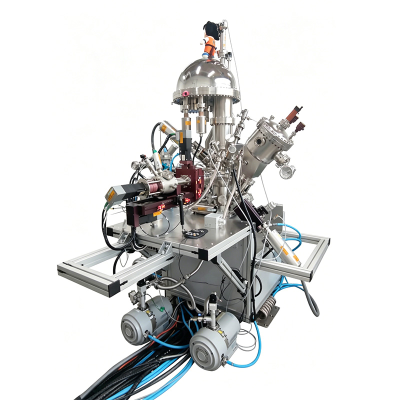
Structure & Key Components
UHV Stainless Steel Vacuum Chamber
Fabricated from high‑quality stainless steel with precise flange sealing design, it achieves excellent air tightness and ultra‑high vacuum level required for thin‑film deposition. The spherical top‑chamber structure optimizes gas flow and film‑forming uniformity.
High‑Efficiency Vacuum Pumping Unit
Equipped with molecular pumps and mechanical pump groups, it rapidly evacuates the chamber to ultra‑high vacuum, effectively removing impurities and ensuring pure thin‑film growth environment.
Precision Sample Transfer & Motion Platform
Custom‑designed multi‑axis precision sample stage supports accurate positioning, rotation and displacement of workpieces. It guarantees consistent coating thickness and outstanding uniformity for small‑batch precision parts.
Complete Sputtering & Auxiliary Systems
Configured with magnetron sputtering cathodes, cooling water circulation system, power supply modules, gas path control units and detection sensors. It stably controls sputtering power, gas flow and working temperature to realize controllable deposition of metal films, alloy films and dielectric films.
- Ultra‑high vacuum design, low‑pollution thin‑film preparation
- High‑precision motion platform for uniform & repeatable coating
- Modular structure, flexible for functional expansion and customization
- Stable power & gas control system for long‑time continuous operation
- Lab‑grade precision, suitable for R&D and small‑batch high‑end production
Applications: